|
Qingdao HNYN Microelectronics Co., Ltd
|
High Temperature Memory With Large Density
| Place of Origin: | , China (Mainland) |
|
|
|
| Add to My Favorites | |
| HiSupplier Escrow |
Product Detail
High Temperature Memory With Large Density,High Temperature Flash Memory 4Gb
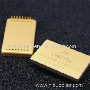
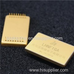
LHNF1GA High temperature memoryIntroduction LHNF1GA is a high temperature and reliable NAND type and commonly used memory, with fast read and write, high reliability characteristics under high and low temperature and can operate continuously under severe environment of -45℃~175℃. Product model Voltage scope Structure Encapsulation LHNF1GA 2.7V~3.6V 1G x 8 bit DIP16 Characteristics Working temperature scope: -45℃~+175℃
The maximum working current: 90mA; standby current: <2mA
Power supply voltage Vcc (V): 2.7V~3.6V
Input high level (V): 0.8Vcc~Vcc+0.3
Input low level (V): -0.3~0.2Vcc
Output high level (V):2.4~Vcc
Output low level (V): -0.3~0.4
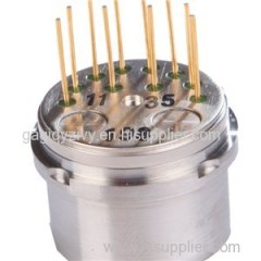
Encapsulation: 16 PIN DIP lead-free encapsulation (45mm x 28mm x 5mm)Pin configurationPin description Pin name Pin function IO0 ~ IO7 Multiplexing I/O Input order, address, input and output data; When chip is not selected or output is invalid, I/O pin is at high impedance state; CLE Command latch enable Enable command is conveyed to register. When CLE is at high level, rising edge of signal, and command through IO port stored into the register.ALE Address latch enable Valid path from enable address to command register. When ALE is at high level, address is latched at the rising edge of.C(—)E(—)Chip enable Component selects control signal. When component is at busy state, high level of C(—)E(—) is ignored; and the component will not return to waiting mode when doing programming or erase operation.R(—)E(—)Read Enable Enable read allows the output of serial data. When the signal is at low level, data is driven to IO port. Data at the falling edge will be valid after R(—)E(—) , and address calculator of internal serial will be increased by 1 automatically.W(—)E(—)Write enable W(—)E(—) inputs write enable to control the input of serial data; Command, address and data latching at the rising edge of W(—)E(—). R/B(—)Ready/Busy output R/B(—) output is used to indicate the operation state of component. When it is at low level, indicating a program, erase or random read is proceeding; when it is at high level, indicating no operation or operation completion, the pin is an open-drain output and will not appear high impedance state when chip is not selected or output unable.Vcc Power supply Vss GroundEncapsulation size and reference picture
Related Search
High Density Polyethylene
High Density Board
High Density Foam
High Density Fabric
High Temperature Resistant
High Temperature Tape
More>>

